
Cabinet Approves India Semiconductor Mission 2.0 with Rs 1.28 Lakh Crore Outlay
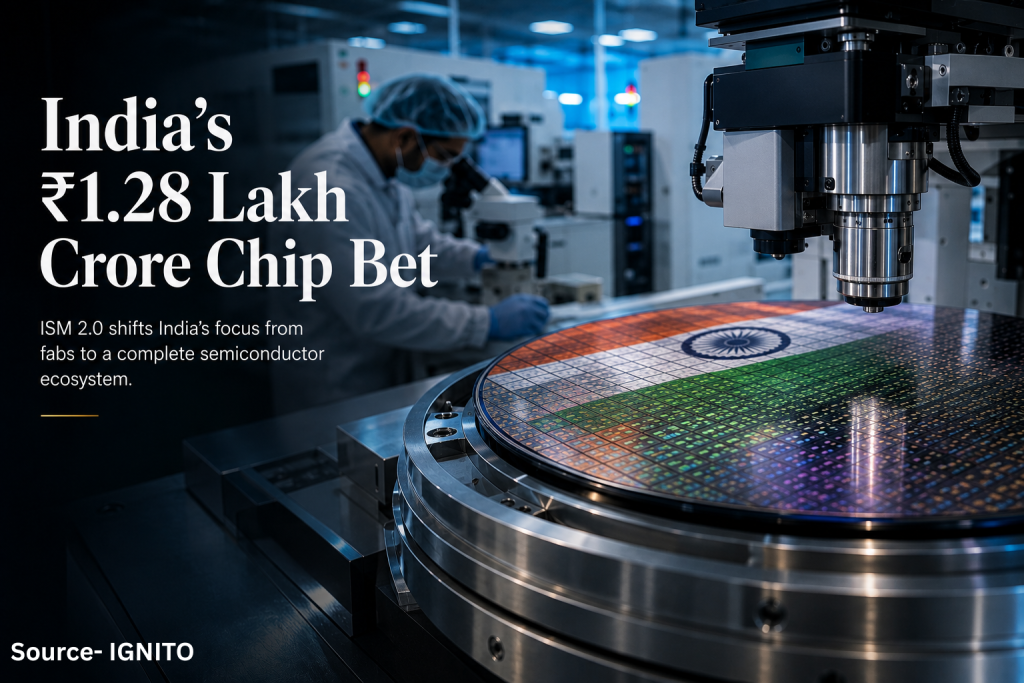
The Union Cabinet approved the India Semiconductor Mission 2.0 (ISM 2.0) with an outlay of Rs 1.28 lakh crore nearly 70% higher than the Rs 76,000 crore allocated under the first phase marking a decisive shift in India’s semiconductor strategy from attracting fabrication plants to building a complete domestic ecosystem spanning equipment, materials, design, research, and talent development.
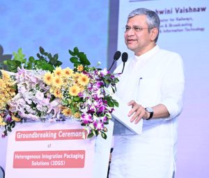
Electronics and IT Minister Ashwini Vaishnaw said the mission’s next phase will prioritise semiconductor design companies and startups, development of the complete manufacturing ecosystem from equipment and materials to testing, expansion of India’s semiconductor talent pool, and a gradual move toward advanced nodes such as 2 nanometres.
ISM 1.0 had already laid a strong foundation, with more than 12 projects approved over four year including Tata Electronics’ semiconductor fab, Micron’s assembly and testing facility, and multiple power semiconductor ventures. The CG Semi OSAT facility inaugurated in Sanand, Gujarat on July 4 stands as one of the most visible outcomes of that first phase, with a production capacity of 5 billion chips annually targeting automotive, industrial, and memory sectors.
ICEA Chairman Pankaj Mohindroo welcomed the Cabinet approval, noting that ISM 1.0 transformed India’s semiconductor ambitions into a tangible manufacturing ecosystem. “ISM 2.0 now builds on this strong foundation with a significant emphasis on design, R&D, capital goods, the entire supply chain, and skill development,” he said, adding that semiconductor design and AI compute based on Indian-owned intellectual property will emerge as key focus areas. He noted that ISM 2.0 can bring together manufacturing, innovation, supply chains, and human capital to build a globally competitive semiconductor ecosystem while encouraging states to compete for fresh investments.