
India Breaks Ground on First Advanced 3D Semiconductor Packaging Unit in Odisha
In a major milestone for India’s semiconductor ambitions, the foundation stone for the country’s first advanced 3D chip packaging unit has been laid at Info Valley, Bhubaneswar, marking a significant step towards strengthening the domestic electronics manufacturing ecosystem.
The project, led by 3D Glass Solutions through its Indian arm Heterogeneous Integration Packaging Solutions Pvt. Ltd., is India’s first facility focused on advanced 3D heterogeneous integration (3DHI) packaging technologies.
The initiative is expected to play a critical role in enabling next-generation technologies such as Artificial Intelligence, high-performance computing, telecommunications, defence electronics, and advanced digital systems.
Speaking at the event, Mohan Charan Majhi described the project as a landmark moment for both Odisha and India, highlighting that the state is emerging as a key destination for advanced semiconductor manufacturing. He noted that Odisha is uniquely positioned as the only state hosting both a compound semiconductor fabrication unit and an advanced 3D glass substrate packaging facility.
The project entails an investment of approximately ₹2,000 crore and is designed to produce around 70,000 glass panels annually, along with 50 million assembled units and nearly 13,000 advanced 3DHI modules. It is expected to generate significant employment opportunities and accelerate the transition of Odisha into a technology-driven economy.
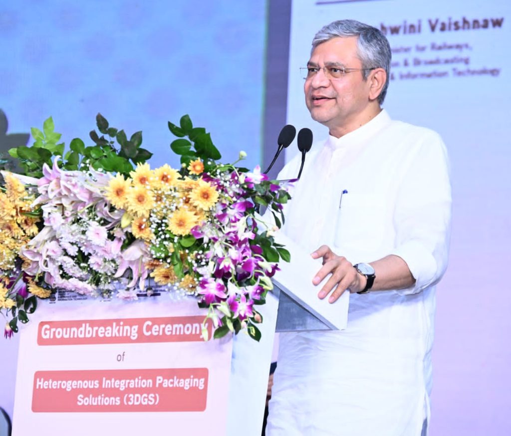
Union Minister Ashwini Vaishnaw emphasised that India’s semiconductor ecosystem is witnessing rapid expansion under the leadership of Prime Minister Narendra Modi. He highlighted that electronics manufacturing in the country has grown six-fold over the past decade, with India now emerging as the world’s second-largest mobile phone manufacturer and a leading exporter.
He further noted that Odisha is becoming an important node in India’s semiconductor journey, with two projects already approved under the India Semiconductor Mission and additional proposals under consideration.
The facility, a greenfield and vertically integrated ATMP (Assembly, Testing, Marking and Packaging) unit, will cater to high-growth sectors including data centres, AI, 5G and 6G communications, automotive systems, aerospace, and photonics.
Commercial production at the unit is expected to commence by August 2028, with full-scale operations targeted by 2030, positioning India as a serious contender in the global semiconductor value chain.
Source : PIB