
Paras Semiconductors to Invest ₹6,200 Crore in Advanced OSAT Facility in Madhya Pradesh, Strengthening India’s Chip Packaging Ecosystem
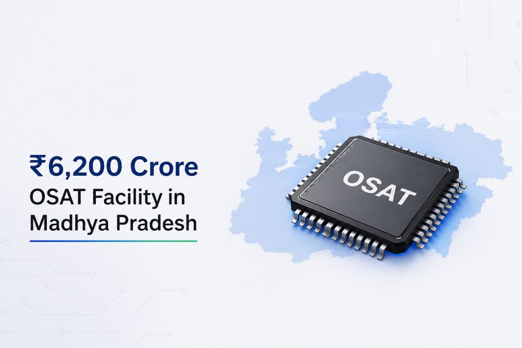
New Delhi: India’s semiconductor ecosystem received another significant boost as Paras Semiconductors announced plans to establish a greenfield Outsourced Semiconductor Assembly and Test (OSAT) facility in Madhya Pradesh with a proposed investment of approximately ₹6,200 crore. The project marks another milestone in the country’s efforts to strengthen domestic semiconductor manufacturing capabilities and develop a globally competitive electronics value chain.
The proposed facility will be developed on nearly 50 acres of land along the Ujjain–Indore industrial corridor, allocated by the Madhya Pradesh government under a Memorandum of Understanding (MoU) signed between the company and the state’s Department of Science and Technology. The strategic location is expected to provide strong logistics connectivity and access to emerging electronics manufacturing clusters.
The OSAT plant will focus on advanced semiconductor packaging technologies, including 3D heterogeneous integration, 2.5D and 3D advanced packaging, hybrid bonding, ultra-high-density fan-out packaging, chiplet integration, wafer bumping, flip-chip assembly, testing, and reliability validation. These technologies are increasingly critical for high-performance computing, artificial intelligence, automotive electronics, telecommunications, defence systems, and next-generation consumer electronics.
According to the company, the facility is intended to address the growing demand for advanced chip packaging while reducing India’s dependence on overseas packaging and testing services. By strengthening domestic back-end semiconductor capabilities, the project complements the country’s broader objective of building a resilient semiconductor supply chain.
The investment also represents a major industrial opportunity for Madhya Pradesh. The project is expected to generate more than 2,500 direct employment opportunities, while creating a much larger ecosystem of indirect jobs across component suppliers, logistics providers, equipment manufacturers, engineering services, and semiconductor support industries.
Industry experts view advanced packaging as one of the fastest-growing segments of the semiconductor industry, with technologies such as chiplet integration and heterogeneous packaging becoming increasingly important for improving chip performance, reducing power consumption, and enabling more compact electronic systems. India’s growing strength in semiconductor design, coupled with investments in packaging and testing, is expected to enhance the country’s competitiveness across the global semiconductor value chain.
The announcement comes amid accelerated policy support for semiconductor manufacturing in India. Recent government initiatives under the India Semiconductor Mission have expanded the focus beyond fabrication to include chip design, advanced packaging, materials, equipment, research, and supply chain development. New investments across multiple states are expected to create an integrated semiconductor ecosystem capable of serving both domestic demand and global markets.
With the proposed OSAT facility, Paras Semiconductors joins a growing list of companies investing in India’s semiconductor infrastructure, reinforcing the country’s ambition to emerge as a trusted global destination for semiconductor manufacturing and advanced electronics production.