
India Scales Chip Design Push, Targets 50 Fabless Firms Under DLI
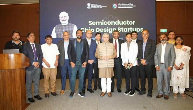
Photo Credit: PIB
Union Minister for Electronics and Information Technology Ashwini Vaishnaw met semiconductor chip design companies supported under the Design Linked Incentive (DLI) Scheme in New Delhi on Tuesday, marking another important step in India’s effort to build a strong and self-reliant semiconductor ecosystem. The interaction focused on reviewing progress made by startups, understanding new design innovations, and reaffirming the government’s long-term commitment to strengthening domestic chip design capabilities under the Semicon India programme.
The DLI Scheme was launched to accelerate India’s indigenous semiconductor design ecosystem by supporting startups and companies working on critical chip technologies. These include system-on-chips, application-specific integrated circuits, telecom and wireless solutions, power management chips, artificial intelligence applications, and Internet of Things products. By lowering entry barriers and offering structured support, the scheme aims to move India beyond services and into high-value product and IP creation.
Companies supported under the scheme are designing a wide range of chips, including indigenous processors for surveillance systems, networking equipment, and embedded platforms. Several startups are working on RISC-V–based processors, AI accelerators, and ultra-low-power chips for edge and IoT use cases. Others are focused on telecom chipsets, mixed-signal and power management ICs, as well as applications in strategic sectors such as automotive, energy, space, railways, and defence. Together, these efforts are helping create a diversified and resilient semiconductor design base in the country.
A key pillar of the programme has been access to advanced electronic design automation tools. Under the scheme, companies and academic institutions have collectively used around 2.25 crore tool-hours. More than 67,000 students and over 1,000 startup engineers are actively engaged in chip design work. Academic institutions have completed 122 tape-outs, with 56 chips fabricated at the 180-nanometre node at SCL Mohali. Startups have achieved 16 tape-outs, leading to six chips being fabricated at advanced nodes, including 12 nanometres. These efforts have also resulted in 75 patents from academia and 10 patents from startups.
Addressing stakeholders, the Minister said the government’s multi-year, ecosystem-led approach is producing measurable results. He recalled that the semiconductor programme was conceived in 2022 with a clear vision from Prime Minister Narendra Modi to build the full value chain, focus on long-term capability, and transform India into a product-driven economy. According to him, the progress achieved so far validates this strategy.
Highlighting the success of the DLI Scheme, the Minister noted that the programme currently supports 24 startups, many of which have already completed tape-outs, validated products, and found early market acceptance. He said the government deliberately focused on removing key constraints faced by startups, such as access to costly tools, IP libraries, and wafer fabrication support. This integrated support framework, he added, is rare even by global standards.
Looking ahead, the government plans to expand the programme and enable at least 50 fabless semiconductor companies in the next phase. The Minister expressed confidence that India will see the rise of globally competitive fabless firms in the coming years, supported by strong design talent, growing market demand, and policy stability.
Sharing insights from recent global discussions, including at the World Economic Forum in Davos, the Minister said international industry leaders now view India’s semiconductor programme as serious, credible, and execution-oriented. Global perception has shifted from early scepticism to active interest in partnerships, co-development, and investment opportunities within India’s semiconductor ecosystem.
The government has identified six priority semiconductor design domains: compute systems, RF and wireless, networking, power management, sensors, and memory. These domains form the core of most modern electronic systems and will enable India to design solutions for a wide range of civilian and strategic applications.
On the manufacturing front, the Minister said SCL Mohali will continue to support 180-nanometre tape-outs, while the upcoming fabrication facility at Dholera will enable advanced nodes up to 28 nanometres. This combination will provide a strong manufacturing backbone to complement domestic design efforts. Talent development remains a parallel focus, with more than 67,000 professionals already trained against a ten-year target of 85,000.
The Minister said that by 2029, India aims to design and manufacture chips for nearly 70 to 75 per cent of its domestic needs. Under Semicon 2.0, the focus will shift toward advanced manufacturing, with a roadmap for 3-nanometre and 2-nanometre technologies. By 2035, India aims to be among the world’s leading semiconductor nations.
Startups under the DLI Scheme have already attracted nearly ₹430 crore in venture capital funding, with 14 of the 24 supported startups securing investments. The Minister also announced that Deep Tech Awards will be instituted in 2026 to recognise excellence in semiconductors, AI, biotechnology, space, and other advanced technologies, further reinforcing India’s innovation-driven growth agenda.
Source: PIB