

ChipIN Centre Drives India’s Semiconductor Vision with Siemens EDA Collaboration
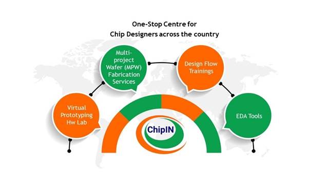
The Government of India, through the Ministry of Electronics and Information Technology (MeitY), is revolutionizing the semiconductor design landscape by empowering the nation’s chip design community. The ChipIN Centre at C-DAC, one of the most advanced semiconductor design facilities, now benefits from extended support by Siemens EDA, accelerating India’s path toward becoming a global semiconductor powerhouse.
Under the Chips to Startup (C2S) Programme, Siemens EDA tools have been made available to over 20,000 students across 250+ academic institutions, with plans to expand access to 85,000 B.Tech, M.Tech, and PhD students within five years. The centre also caters to entrepreneurs and start-ups, offering end-to-end solutions, including access to state-of-the-art Electronic Design Automation (EDA) tools, hardware infrastructure, and IP cores.
Siemens has extended the use of its Veloce™ hardware-assisted verification solution to companies approved under MeitY’s Design Linked Incentive (DLI) Scheme. Veloce’s advanced features, including 128 CPU cores and a capacity of 640 million gates, address critical SoC and IC design challenges.
Sunita Verma, Group Coordinator at MeitY, emphasized the initiative’s role in building a self-reliant semiconductor ecosystem, while Siemens’ Ruchir Dixit highlighted its commitment to empowering India’s next generation of engineers and researchers to drive technological innovation.
Source: PIB